rent-now

Rent More, Save More! Use code: ECRENTAL

5% off 1 book, 7% off 2 books, 10% off 3+ books

9780134670904

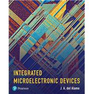
Integrated Microelectronic Devices Physics and Modeling

by
  • ISBN13:

    9780134670904

  • ISBN10:

    0134670906

  • Edition: 1st
  • Format: Hardcover
  • Copyright: 2017-01-20
  • Publisher: Pearson

Note: Supplemental materials are not guaranteed with Rental or Used book purchases.

Purchase Benefits

  • Free Shipping Icon Free Shipping On Orders Over $35!
    Your order must be $35 or more to qualify for free economy shipping. Bulk sales, PO's, Marketplace items, eBooks and apparel do not qualify for this offer.
  • eCampus.com Logo Get Rewarded for Ordering Your Textbooks! Enroll Now
  • Complimentary 7-Day eTextbook Access - Read more
    When you rent or buy this book, you will receive complimentary 7-day online access to the eTextbook version from your PC, Mac, tablet, or smartphone. Feature not included on Marketplace Items.
List Price: $239.98 Save up to $161.99
  • Rent Book $170.98
    Add to Cart Free Shipping Icon Free Shipping

    TERM
    PRICE
    DUE

    7-Day eTextbook Access 7-Day eTextbook Access

    USUALLY SHIPS IN 2-3 BUSINESS DAYS
    *This item is part of an exclusive publisher rental program and requires an additional convenience fee. This fee will be reflected in the shopping cart.

How To: Textbook Rental

Looking to rent a book? Rent Integrated Microelectronic Devices Physics and Modeling [ISBN: 9780134670904] for the semester, quarter, and short term or search our site for other textbooks by del Alamo, J. A.. Renting a textbook can save you up to 90% from the cost of buying.

Summary

A modern take on microelectronic device engineering

Microelectronics is a 50-year-old engineering discipline still undergoing rapid evolution and societal adoption. Integrated Microelectronic Devices: Physics and Modeling fills the need for a rigorous description of semiconductor device physics that is relevant to modern nanoelectronics. The central goal is to present the fundamentals of semiconductor device operation with relevance to modern integrated microelectronics. Emphasis is devoted to frequency response, layout, geometrical effects, parasitic issues and modeling in integrated microelectronics devices (transistors and diodes). In addition to this focus, the concepts learned here are highly applicable in other device contexts.


This text is suitable for a one-semester junior or senior-level course by selecting the front sections of selected chapters (e.g. 1-9). It can also be used in a two-semester senior-level or a graduate-level course by taking advantage of the more advanced sections. 

Author Biography

Jesús A. del Alamois Donner Professor and Professor of Electrical Engineering in the Department of Electrical Engineering and Computer Science at Massachusetts Institute of Technology. He is also Director of the Microsystems Technology Laboratories at MIT. He obtained a Telecommunications Engineer degree from the Universidad Politécnica de Madrid (Spain) and MS and PhD degrees in Electrical Engineering from Stanford University. Over the years, Prof. del Alamo has been involved in research on transistors and other electronic devices in a variety of material systems. He has worked on Si solar cells, Si bipolar junction transistors, Si metal—oxide—semiconductor field-effect transistors (MOSFETs), SiGe heterostructure devices, GaAs pseudomorphic high electron mobility transistors (PHEMTs), InGaAs high electron mobility transistors (HEMTs) and MOSFETs, InGaSb HEMTs and MOSFETs, GaN HEMTs and MOSFETs, and more recently diamond MOSFETs. Prof. del Alamo teaches undergraduate and graduate-level courses at MIT in electronics, electron devices and circuits, and advanced semiconductor device physics. He has received multiple teaching and achievement awards at MIT: the 1992 Baker Memorial Award for Excellence in Undergraduate Teaching, the 1993 H. E. Edgerton Junior Faculty Achievement Award, the 2001 Louis D. Smullin Award for Excellence in Teaching, and the 2002 Amar Bose Award for Excellence in Teaching. In 2012, Prof. del Alamo was awarded the IEEE Electron Devices Society Education Award “for pioneering contributions to the development of online laboratories for microelectronics education on a worldwide scale”.

Table of Contents

Preface xv


About the Author xix


1 Electrons, Photons, and Phonons


1.1 Selected Concepts of Quantum Mechanics


1.1.1 The dual nature of the photon


1.1.2 The dual nature of the electron


1.1.3 Electrons in confined environments


1.2 Selected Concepts of Statistical Mechanics


1.2.1 Thermal motion and thermal energy


1.2.2 Thermal equilibrium


1.2.3 Electron statistics


1.3 Selected Concepts of Solid-State Physics


1.3.1 Bonds and bands


1.3.2 Metals, insulators, and semiconductors


1.3.3 Density of states


1.3.4 Lattice vibrations: phonons


1.4 Summary


1.5 Further reading


Problems


2 Carrier Statistics in Equilibrium


2.1 Conduction and Valence Bands; Bandgap; Holes


2.2 Intrinsic Semiconductor


2.3 Extrinsic Semiconductor


2.3.1 Donors and acceptors


2.3.2 Charge neutrality


2.3.3 Equilibrium carrier concentration in a doped semiconductor


2.4 Carrier Statistics in Equilibrium


2.4.1 Conduction and valence band density of states


2.4.2 Equilibrium electron concentration


2.4.3 Equilibrium hole concentration


2.4.4 np product in equilibrium


2.4.5 Location of Fermi level


2.5 Summary


2.6 Further Reading


Problems


3 Carrier Generation and Recombination


3.1 Generation and Recombination Mechanisms


3.2 Thermal Equilibrium: Principle of Detailed Balance


3.3 Generation and Recombination Rates in Thermal Equilibrium


3.3.1 Band-to-band optical generation and recombination


3.3.2 Auger generation and recombination


3.3.3 Trap-assisted thermal generation and recombination


3.4 Generation and Recombination Rates Outside Equilibrium


3.4.1 Quasi-neutral low-level injection; recombination lifetime


3.4.2 Extraction; generation lifetime


3.5 Dynamics of Excess Carriers in Uniform Situations


3.5.1 Example 1: Turn-on transient


3.5.2 Example 2: Turn-off transient


3.5.3 Example 3: A pulse of light


3.6 Surface Generation and Recombination


3.7 Summary


3.8 Further Reading


Problems


4 Carrier Drift and Diffusion


4.1 Thermal Motion


4.1.1 Thermal velocity


4.1.2 Scattering


4.2 Drift


4.2.1 Drift velocity


4.2.2 Velocity saturation


4.2.3 Drift current


4.2.4 Energy band diagram under electric field


4.3 Diffusion


4.3.1 Fick’s first law


4.3.2 The Einstein relation


4.3.3 Diffusion current


4.4 Transit Time


4.5 Nonuniformly Doped Semiconductor in Thermal Equilibrium


4.5.1 Gauss’ law


4.5.2 The Boltzmann relations


4.5.3 Equilibrium carrier concentration


4.6 Quasi-Fermi Levels and Quasi-Equilibrium


4.7 Summary


4.8 Further Reading


Problems


5 Carrier Flow


5.1 Continuity Equations


5.2 Surface Continuity Equations


5.2.1 Free surface


5.2.2 Ohmic contact


5.3 Shockley Equations


5.4 Simplifications of Shockley Equations to One-Dimensional Quasi-Neutral


Situations


5.5 Majority-Carrier Situations


5.5.1 Example 1: Semiconductor bar under voltage


5.5.2 Example 2: Integrated resistor


5.6 Minority-Carrier Situations


5.6.1 Example 3: Diffusion and bulk recombination in a “long” bar


5.6.2 Example 4: Diffusion and surface recombination in a “short” bar


5.6.3 Length scales of minority carrier situations


5.7 Dynamics of Majority-Carrier Situations


5.8 Dynamics of Minority-Carrier Situations


5.8.1 Example 5: Transient in a bar with S = ∞


5.9 Transport in Space-Charge and High-Resistivity Regions


5.9.1 Example 6: Drift in a high-resistivity region under external


electric field


5.9.2 Comparison between SCR and QNR transport


5.10 Carrier Multiplication and Avalanche Breakdown


5.10.1 Example 7: Carrier multiplication in a high-resistivity region


with uniform electric field


5.11 Summary


5.12 Further Reading


Problems


6 PN Junction Diode


6.1 The Ideal PN Junction Diode


6.2 Ideal PN Junction in Thermal Equilibrium


6.3 Current–Voltage Characteristics of The Ideal PN Diode


6.3.1 Electrostatics under bias


6.3.2 I–V characteristics: qualitative discussion


6.3.3 I–V characteristics: quantitative models


6.4 Charge–Voltage Characteristics of Ideal PN Diode


6.4.1 Depletion charge


6.4.2 Minority carrier charge


6.5 Equivalent Circuit Models of The Ideal PN Diode


6.6 Nonideal and Second-Order Effects


6.6.1 Short diode


6.6.2 Space-charge generation and recombination


6.6.3 Series resistance


6.6.4 Breakdown voltage


6.6.5 Nonuniform doping distributions


6.6.6 High-injection effects


6.7 Integrated PN Diode


6.7.1 Isolation


6.7.2 Series resistance


6.7.3 High–low junction


6.8 Summary


6.9 Further Reading


Problem


7 Schottky Diode and Ohmic Contact


7.1 The Ideal Schottky Diode


7.2 Ideal Schottky Diode in Thermal Equilibrium


7.2.1 A simpler system: a metal–metal junction


7.2.2 Energy band lineup of metal–semiconductor junction


7.2.3 Electrostatics of metal–semiconductor junction in equilibrium


7.3 Current–Voltage Characteristics of Ideal Schottky Diode


7.3.1 Electrostatics under bias


7.3.2 I–V characteristics: qualitative discussion


7.3.3 I–V characteristics: thermionic emission model


7.4 Charge–Voltage Characteristics of Ideal Schottky Diode


7.5 Equivalent Circuit Models for The Ideal Schottky Diode


7.6 Nonideal and Second-Order Effects


7.6.1 Series resistance


7.6.2 Breakdown voltage


7.7 Integrated Schottky Diode


7.8 Ohmic Contacts


7.8.1 Lateral ohmic contact: transmission-line model


7.8.2 Boundary conditions imposed by ohmic contacts


7.9 Summary


7.10 Further Reading


Problems


8 The Si Surface and the Metal–OxideSemiconductor Structure


8.1 The Semiconductor Surface


8.2 The Ideal Metal–Oxide–Semiconductor Structure


8.3 The Ideal Metal–Oxide–Semiconductor Structure at Zero Bias


8.3.1 General relations for the electrostatics of the ideal MOS structure


8.3.2 Electrostatic of the MOS structure under zero bias


8.4 The Ideal Metal–Oxide Semiconductor Structure Under Bias


8.4.1 Depletion


8.4.2 Flatband


8.4.3 Accumulation


8.4.4 Threshold


8.4.5 Inversion


8.4.6 Summary of charge–voltage characteristics


8.5 Dynamics of The MOS Structure


8.5.1 Quasi-static C–V characteristics


8.5.2 High-frequency C–V characteristics


8.5.3 Deep depletion


8.6 Weak Inversion and The Subthreshold Regime


8.7 Three-Terminal MOS Structure


8.8 Summary


8.9 Further Reading


Problems


9 The “Long” Metal–Oxide–Semiconductor Field-Effect Transistor


9.1 The Ideal MOSFET


9.2 Qualitative Operation of The Ideal MOSFET


9.3 Inversion Layer Transport in The Ideal MOSFET


9.4 Current–Voltage Characteristics of The Ideal MOSFET


9.4.1 The cut-off regime


9.4.2 The linear regime


9.4.3 The saturation regime


9.4.4 DC large-signal equivalent-circuit model of ideal MOSFET


9.4.5 Energy band diagrams


9.5 Charge–Voltage Characteristics of The Ideal MOSFET


9.5.1 Depletion charge


9.5.2 Inversion charge


9.6 Small-Signal Behavior of Ideal MOSFET


9.6.1 Small-signal equivalent circuit model of ideal MOSFET


9.6.2 Short-circuit current-gain cut-off frequency, fT, of ideal MOSFET


in saturation


9.7 Nonideal Effects in MOSFET


9.7.1 Body effect


9.7.2 Effect of back bias


9.7.3 Channel-length modulation


9.7.4 The subthreshold regime


9.7.5 Source and drain resistance


9.8 Summary


9.9 Further Reading


Problems


10 The “Short” Metal–Oxide–Semiconductor Field-Effect Transistor


10.1 MOSFET Short-Channel Effects: Transport


10.1.1 Mobility degradation


10.1.2 Velocity saturation


10.2 MOSFET Short-Channel Effects: Electrostatics


10.2.1 Threshold voltage dependence on gate length: VT rolloff


10.2.2 Threshold voltage dependence on VDS: drain-induced barrier


lowering (DIBL)


10.2.3 Subthreshold swing dependence on gate length and VDS


10.3 MOSFET Short-Channel Effects: Gate Stack Scaling


10.3.1 Gate capacitance


10.3.2 Gate leakage current


10.4 MOSFET High-Field Effects


10.4.1 Electrostatics of velocity saturation region


10.4.2 Impact ionization and substrate current


10.4.3 Output conductance


10.4.4 Gate-induced drain leakage


10.5 MOSFET Scaling


10.5.1 The MOSFET as a switch


10.5.2 Constant field scaling of the ideal MOSFET


10.5.3 Constant voltage scaling of the ideal MOSFET


10.5.4 Generalized scaling of short MOSFETs


10.5.5 MOSFET scaling: a historical perspective


10.5.6 Evolution of MOSFET design


10.6 Summary


10.7 Further Reading


Problems


11 The Bipolar Junction Transistor


11.1 The Ideal BJT


11.2 Current–Voltage Characteristics of The Ideal BJT


11.2.1 The forward-active regime


11.2.2 The reverse regime


11.2.3 The cut-off regime


11.2.4 The saturation regime


11.2.5 Output I–V characteristics


11.3 Charge–Voltage Characteristics of Ideal BJT


11.3.1 Depletion charge


11.3.2 Minority carrier charge


Supplemental Materials

What is included with this book?

The New copy of this book will include any supplemental materials advertised. Please check the title of the book to determine if it should include any access cards, study guides, lab manuals, CDs, etc.

The Used, Rental and eBook copies of this book are not guaranteed to include any supplemental materials. Typically, only the book itself is included. This is true even if the title states it includes any access cards, study guides, lab manuals, CDs, etc.

Rewards Program